Hong Kong Is Building Its First Third-generation Semiconductor Gallium Nitride Epitaxial Wafer Pilot Line
Published: 8.9.2024
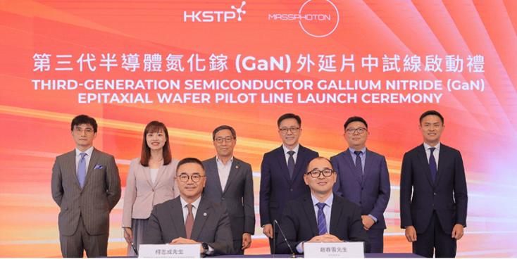
On July 30, the Hong Kong Science and Technology Park Corporation (HKSTP) and MassPhoton jointly held the launch ceremony of Hong Kong's first ultra-high vacuum "third-generation semiconductor gallium nitride (GaN) epitaxial wafer pilot line". This event not only marks that Hong Kong has taken solid steps in the field of microelectronics industry, but also symbolizes that Hong Kong has achieved a new milestone in the process of new industrialization.
According to the data, as the largest innovation and technology flagship in Hong Kong, the Hong Kong Science and Technology Park Corporation has been committed to promoting technological innovation and industrial development. The Science and Technology Park Corporation provides first-class infrastructure and a large network of partners, providing strong support for the research and development and industrialization of the microelectronics industry. At present, the Science and Technology Park has gathered more than 200 companies engaged in the microelectronics industry, forming a vibrant microelectronics ecosystem.
MassPhoton Technology is a high-tech enterprise focusing on gallium nitride epitaxial technology. The company was founded by Dr. Liao Yitao, an expert with more than 40 patented technologies in the fields of GaN epitaxy and deep ultraviolet LED devices, and the founding team is composed of senior returnees. Technical personnel. According to the company's website, the company is headquartered in Shenzhen, with a branch in Hong Kong, a production base in Xuzhou, and a light science and disinfection technology laboratory at Boston University in the United States.
The ultra-high vacuum "third-generation semiconductor gallium nitride epitaxial wafer pilot line" launched this time is the first 8-inch GaN epitaxial wafer production line in Hong Kong, and is expected to invest at least HK$200 million. It is expected that after the project is completed in 2027, it will achieve an annual production capacity of 10,000 8-inch gallium nitride wafers, providing high-quality epitaxial wafer products for the global market. In addition, Massachusetts Photonics Technology also plans to set up a global R&D center in Hong Kong Science Park and carry out cutting-edge third-generation semiconductor R&D projects with Hong Kong universities and other partners.
Third-generation semiconductor materials, such as gallium nitride and silicon carbide, have become a research hotspot in the global semiconductor industry due to their significant advantages in energy efficiency, volume and operating temperature range. As one of the main representative materials of third-generation semiconductors, gallium nitride has the characteristics of wide bandgap, high frequency, low loss, strong radiation resistance and excellent breakdown electric field. Compared with traditional silicon-based semiconductors, gallium nitride has higher energy efficiency and smaller size, and is suitable for high-speed, high-power and high-frequency applications such as wireless communications, fast charging, industry and automobile fields.
It is estimated that by 2026, the global gallium nitride power component market will reach US$1.33 billion, with a compound growth rate of 65%. By building the first GaN epitaxial wafer pilot line, Hong Kong will not only enhance its own scientific and technological innovation capabilities, but also occupy an important position in the global semiconductor supply chain.


