
At one point, industry insiders were highly skeptical that such a chip could be delivered to market so soon, yet with the help of Dutch Semiconductor company ASML, this vision is finally being realized and ready to take off. In pioneering a way to carve out circuitry patterns into silicon through a process known as extreme ultraviolet (EUV) lithography, ASML has been able to develop a “five nanometer process” that refers to the premise that the chips’ transistors have been effectively shrunk where the miniscule on-off switches are now only around 25 atoms wide, meaning that billions more can be packed in. Simplified, what this process means is that with this 5nm chip, smartphones will now have even more brain power, powering these new smartphones in ways never seen before.
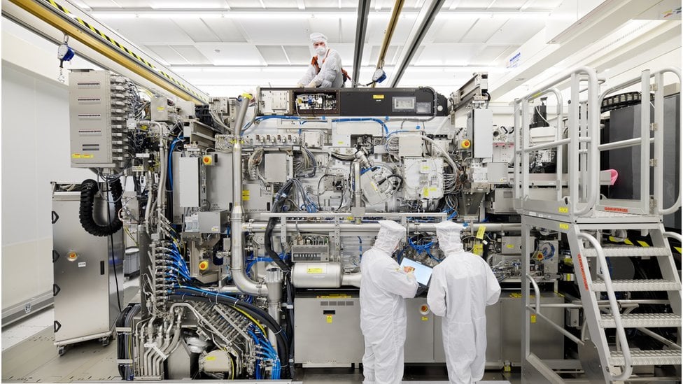
While ASML’s machines cost $123 million (£92 million), which seems exorbitant even in comparison to other similar semiconductor tools used throughout the industry, ASML are still the only company on the planet currently producing these chips. Paired with a low defect rate that also makes these chips more cost-effective than going with other company’s at moment’s time, and it’s no wonder that ASML has been able to partner with Apple on production of the new iPhone.
As stated by Dr. Ian Cutress who reports on the sector for Anandtech, “At such small scales precision is key,” where he then continues to make note that “What they’re doing is akin to hitting a stamp on the surface of Mars with a paper aeroplane.” In fact, ASML compares their technology to making the step forward from the use of a marker pen to a fine-liner, yet instead of using ink in this case, ASML is using what the company has dubbed as “feeble light” through a truly mind-boggling process.
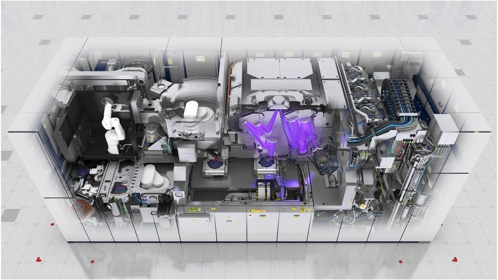
A further look at how ASML utilizes extreme ultraviolet light is explained further by spokesman Sander Hofman who describes the process in claiming “We take a molten droplet of tin and we fire a high-power industrial laser onto it, which basically vaporizes it and creates a plasma,” where “that plasma shines UV light.” According to Hofman “This all happens 50,000 times a second – so 50,000 droplets get hit – which creates enough light for us to capture with a series of mirrors – the flattest in the world.” Hofman also makes note of how a blueprint of the chip’s design is encoded into the light in passing it through a mask where they then begin to shrink it with lenses. From there, it then hits a light-sensitive coating on a silicon wafer which causes the chip’s design to be effectively “printed.”
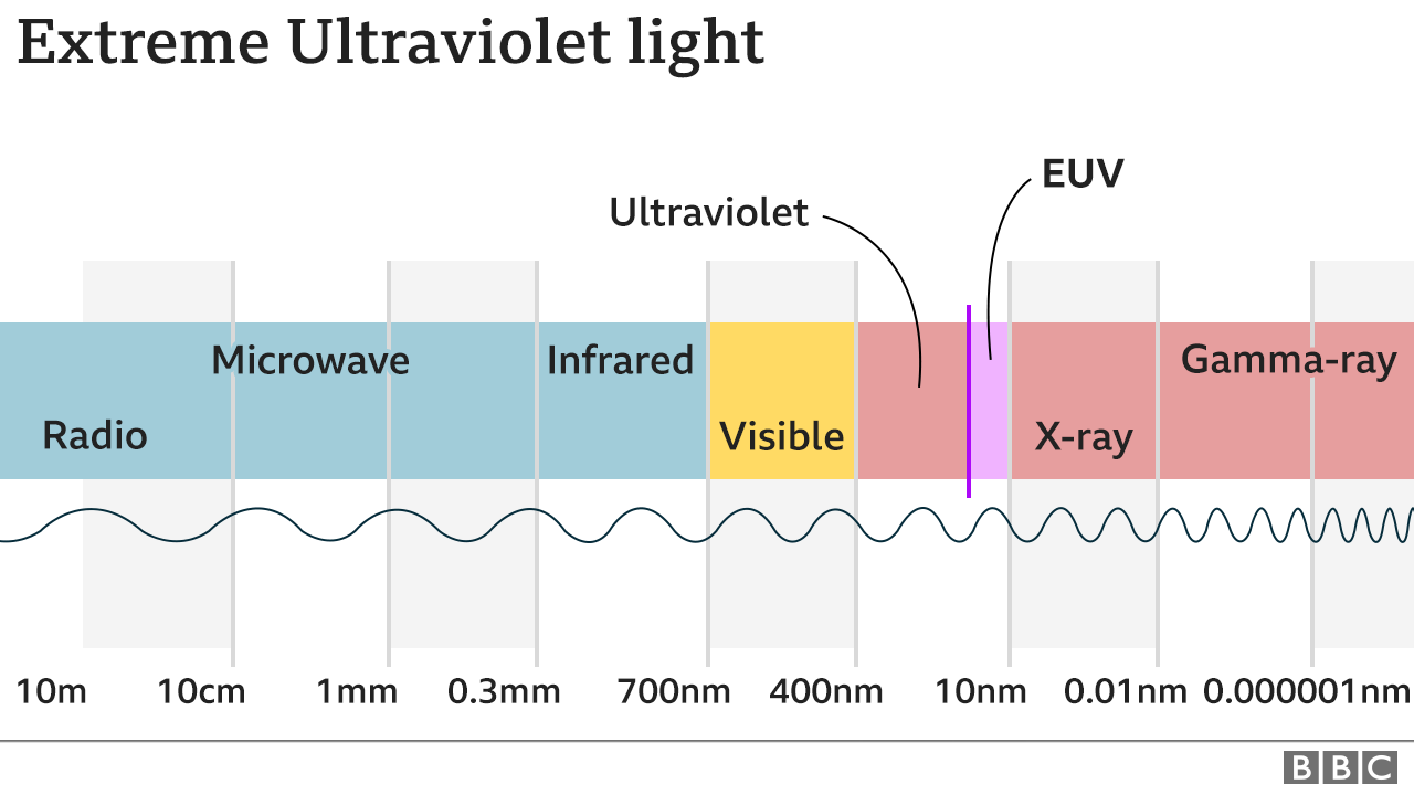
To get a further idea of what exactly this 5 nanometer sized chip means, it is best to first start off by explaining what a nanometer exactly is. A nanometer is one billionth of a meter, which is approximately the speed that a human hair grows per second. Once upon a time, transistors used to be measured with respects to the width of a part referred to as their “gate,” yet it is with this said that around a decade ago the nanometer reference was finally not tied to a single geometry, revolutionizing the way these chips were designed and produced. Illustrating just how small these new transistors are, there are approximately 171 million transistors laid out across every square millimeter. In the present, it is apparent that these 5nm chips are critical in making our smartphones/devices even smarter. Yet, the possibilities and opportunities that can unfold as a result of this chip are truly endless, making complex “artificial intelligence” jobs possible and allowing for smartphones to better understand the world around them. As more brands are expected to follow suit and move to the 5nm chip, eventually one day even unveiling 3nm technological capabilities, this product is one that is set to change the trajectory path of industries and companies across the globe, far beyond the scope of smartphones.
Why We Are One
For over 40 years, IBS Electronics Group has provided a broad range of integrated supply chain and electronicsmanufacturing solutions tailored specific to our customer's operations. As your one source for the industry’s top brands all in one place, our engineers specialize in reducing supply chain complexity and are here to provide you with dedicated support from prototype to production.


.png?resizemode=force&maxsidesize=96)